Overview of the Project
A basic CPU implementation, designed in Verilog. The CPU has enough opcodes to allow for the execution of pretty much any algorithm.
The CPU has three states that it will cycle through for each instruction. To make programming more practical, I also created a custom assembly language with a Python parser that converts the assembly code into 16-bit machine code for the CPU to execute.
This is my final project for Digital System Design (ELEC 4200), and is on GitHub
Software Used for Development
- Xilinx Vivado for Verilog RTL design and simulation
- Python for the custom assembly language parser
Features
Architecture
- 32-bit registers
- 16-bit instruction width
- 16 general-purpose registers
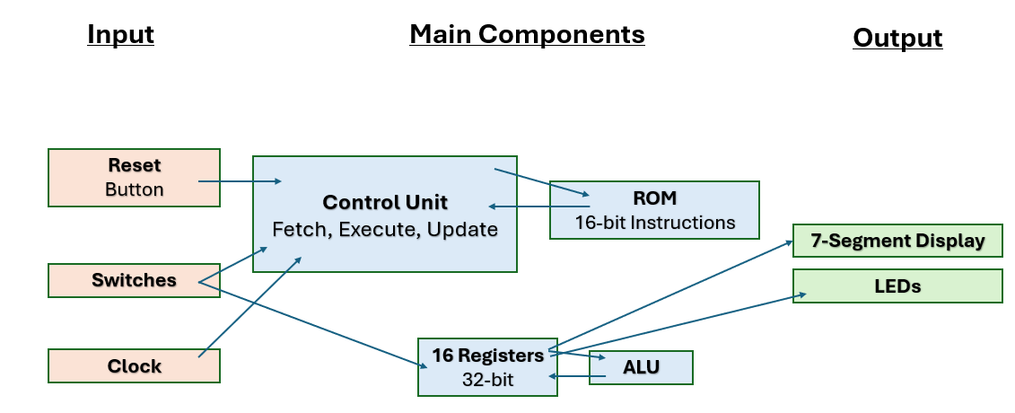
The block diagram of the CPU is shown below:

Opcodes
opcodes = {
    'mov': '000',
    'load': '001',
    'alu': '010',
    'save_alu': '011',
    'load_input': '100',
    'branch_if_zero': '101',
    'end': '111'
}
With only these opcodes, almost any algorithm can be executed.
Limitations
- Maximum program size is 256 lines
LOADinstruction can only input 8-bit values (despite 32-bit registers)
CPU States
The CPU cycles through three states:
FETCH: The current_instruction register is set, based on the program counter.
EXECUTE: The current instruction is executed. This is basically a case statement that executes based on the opcode.
UPDATE: This state increments the program counter and sets outputs (such as 7-segment display).
This means it takes 3 clock cycles per instruction. This could probably be optimized through pipelining.
Custom Assembly Langauge
The CPU takes in 16-bit instructions. The first bits, 15-13, are the opcode.
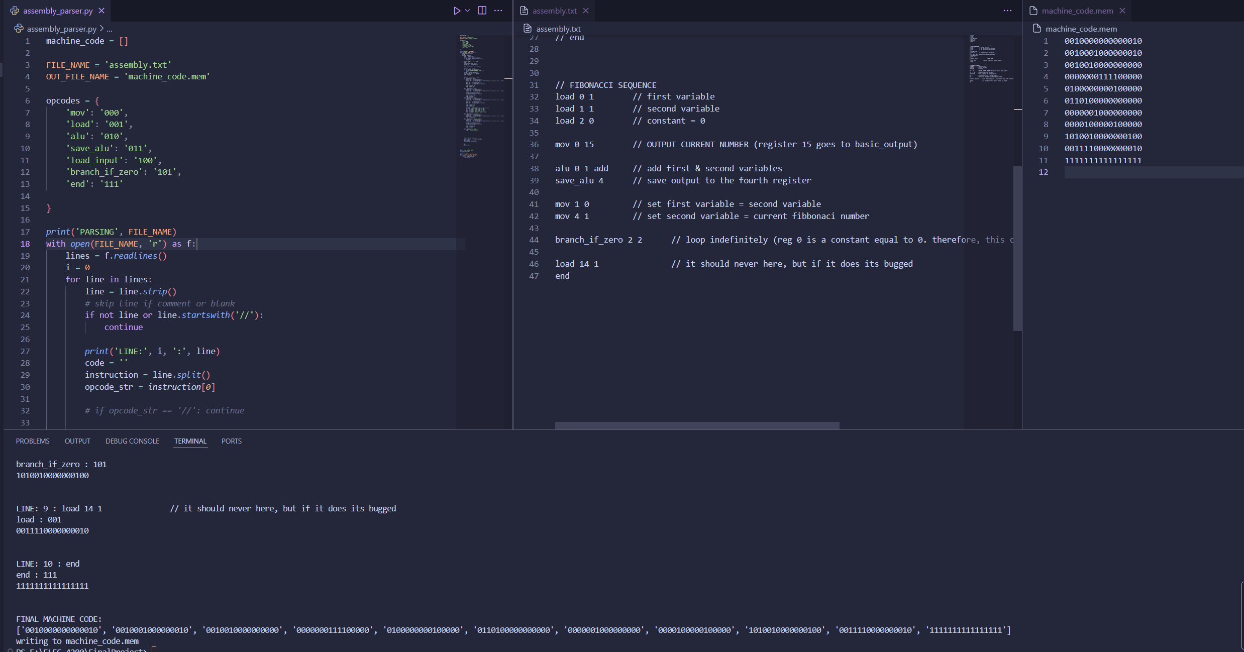
To make programming the CPU easier, I made a Python script to parse the assembly language to machine code:
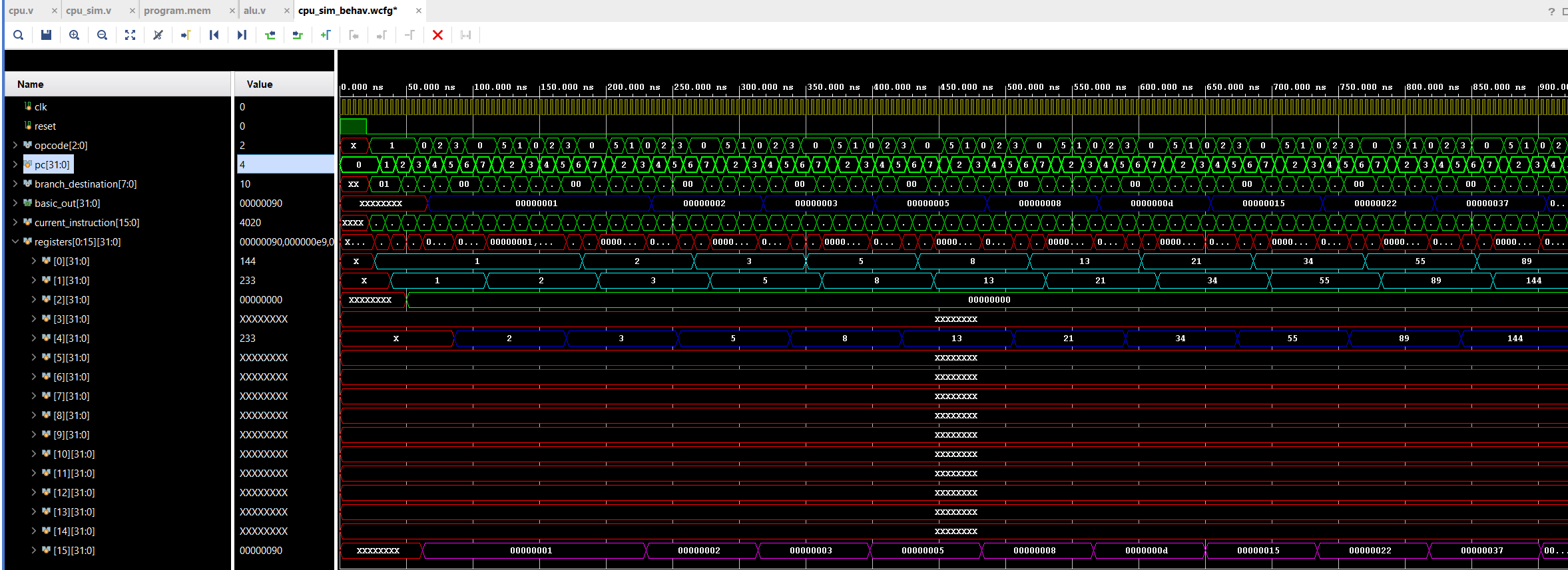
 This program will output the fibonacci sequence.
 Registers 0 and 1 hold the numbers to be added together. We can see these registers advance through the fibonacci sequence. This program will loop forever.
ALU
The ALU is a separate module that is instantiated by the CPU:
module alu #(parameter WIDTH = 32)(
    input [2:0] alu_mode,
    input [WIDTH-1:0] alu_in1, alu_in2,
    output reg [WIDTH-1:0] alu_out
);
The ALU has many modes:
- Addition
- Subtraction
- Multiplication
And logic operations: - Equals
I'm going to add more ALU modes later
The ALU can be interfaced with assembly code:
alu 0 1 add // add register 0 and register 1
The output can then be saved to a register:
save_alu 4 // save alu_out to register 4
After these two assembly lines, the sum of registers 0 and 1 will be saved to register 4.
FPGA Integration
For the final project, I also am required to run this CPU on hardware. Testing the CPU operation on the FPGA required significant debugging due to how Vivado synthesizes and implements Verilog code. One major challenge was configuring the 7-segment display clock. The display cycles through digits rapidly to appear continuously lit, which required creating a separate clock divider to control the switching speed.
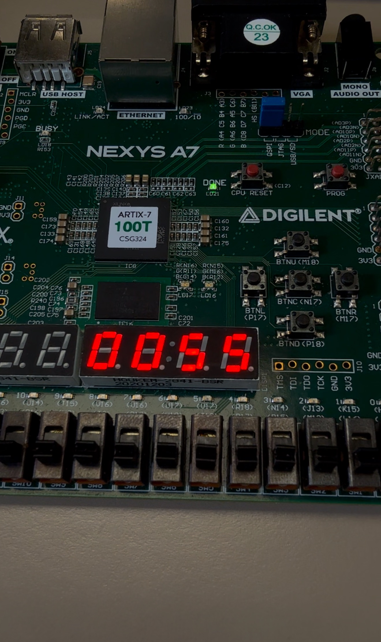
Vivado's synthesis process initially caused unexpected issues with the display's operation. After resolving these, the CPU worked flawlessly, successfully running programs like a counter, the Fibonacci sequence, and addition using switch inputs. Below, the 7-segment display shows the 11th Fibonacci number, 55, as proof of the working design.

Final Project Report
The final project required a report to summarize my work.